High voltage amplifiers: so you think you have noise!
Falco Systems application note, version 1.0, March 2016
W. Merlijn van Spengen, PhD
Introduction
In this application note we discuss noise and interference issues related to the use of high voltage amplifiers. Many of the concepts discussed here are equally applicable to other forms of precision measurements, such as those with low voltage preamplifiers, or I/V-converters (current-to voltage or transimpedance amplifiers). High voltage amplifiers are often used as e.g. piezo drivers or for steering MEMS (micro-electromechanical systems) devices. In many applications, the noise specifications of the high voltage amplifier are of paramount importance, as the output noise directly translates into position noise/uncertainty of the piezo or MEMS actuator that comprises the load of the amplifier.
In the first half of this application note, we cover basic properties of random electronic noise, and how to interpret specifications properly. We also have a look at various ways manufacturers can 'beef up' their amplifier noise specifications, so that an informed choice for the most suitable amplifier for a specific application can be made. In the second half of this application note, we discuss typical interference mechanisms (often also called 'noise', just to confuse everyone around), and the effects that interference can have on low noise measurements. We will see ways to mitigate interference, and provide 'optimal' measurement solutions that reject the different types of interference as much as possible.
Section 1 - Noise
Random electronic noise - a little bit of theory
Noise voltages are defined as the fluctuations a certain value, the noiseless signal voltage. These fluctuations typically have a Gaussian amplitude distribution, with small deviations being much more likely than large ones (Fig 1). As the maximum peak-to-peak excursions of the noise voltage are statistically ill defined, we typically use the root mean square (rms) voltage noise to quantify the amount of noise. The rms value corresponds to one standard deviation in statistics. The typical observable peak-to-peak values of the noise are 6 - 8 times the rms value.
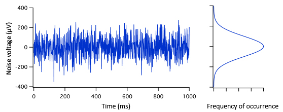
Figure 1. Electronic noise example
Electronic noise is found almost everywhere where precision measurements are made. The two basic types of electronic noise are thermal (also called Johnson) noise and shot noise. In addition, al relatively low frequencies, one often encounters 1/f noise, a type of noise of which the power (not the voltage) rises with one over the frequency f if one looks at lower and lower frequencies. The latter is typically caused by imperfections of the manufacturing process of electronics components, and as such it is less fundamental than the first two.
Thermal noise is a basic fact of physics, and finds its roots in the fluctuation-dissipation theorem. Any physical system with dissipation shows this noise: not only resistors (which are an obvious class of 'dissipative' elements in electronics), but also e.g. mechanical systems with damping show this noise. As such it manifests itself in fields as diverse as electronics, laser frequency stability and Brownian motion. It also sets the ultimate limit on AFM (atomic force microscope) cantilever resolution.
In electronics, the amount of rms thermal noise voltage v_n in Volts is given by v_n=sqrt(4kTRB), where k is the Boltzmann constant (k = 1.38*10^-23 J/K), T is the absolute temperature in Kelvin, R is the resistance in Ohms, and B is the bandwidth of the system (in Hz). Thermal noise is lowered when the temperature, resistance and/or bandwidth of the system are reduced, and therefore sensitive detectors are often cooled with liquid nitrogen or even liquid helium.
As an example, the thermally induced rms noise voltage across the terminals of a 1 Ohm resistor in a 1 Hz bandwidth at room temperature is v_n = sqrt((1.38*10^(-23)*293*1*1)) = 0.127 nV. If the resistance is higher, the noise will rise with the square root of this resistance (so that it becomes e.g. 1.27 nV for 100 Ohm). It will also rise with the square root of the bandwidth, if the bandwidth is increased (so that is becomes e.g. 12.7 nV for 100 Ohm in a 100 Hz bandwidth). As the bandwidth of a system is often not known a priori, thermal noise is often expressed as a number with unit nV/sqrt(Hz), indicating that the rms noise voltage is obtained if this value is multiplied by the square root of the bandwidth of the system.
Shot noise appears everywhere in the world where discrete particles cross an energy barrier one by one. In electronics, it appears when electrons independently cross a semiconductor junction, such as in diodes and transistors (or free space in an electron tube). Many people are also familiar with the 'grainy-ness' of a photographic image taken under low light conditions, which is caused by the discreteness of light particles: photons also have shot noise.
In electronics the noisiness (fluctuations) of a current flowing across a barrier is given as the rms current noise in in Ampere, given by i_n = sqrt(2qIB), where q is the elementary charge (q = 1.60*10^19 C), I is the steady DC current in Ampere flowing across the barrier, and B is the bandwidth of the system in Hz, just like in the thermal noise case. This equation then gives rise to a value for the current noise which typically has the unit pA/sqrt(Hz) or nA/(sqrt(Hz), where again one has to multiply this value by the square root of the bandwidth to obtain the total rms current noise present in a system with a certain bandwidth.
Both thermal noise and current noise are white, meaning that there is equal noise power at every frequency: the noise spectrum is flat. Only if this is the case, multiplying by the square root of the bandwidth will result in the correct total noise. In fact, what you have to do is taking the integral over the noise spectrum.
The 1/f noise is much less well defined. Different components that at first appear to have the same specifications (e.g. they have the same resistance and bandwidth) can have wildly differing 1/f noise, even if they come from the same batch. The only way to get a good understanding of the 1/f noise in a system is to actually measure it.
Basic noise evaluation of high voltage amplifiers
The manufacturer of a low noise high voltage amplifier will have taken considerable care that both thermal noise contributions of components and current noise contributions in the amplifier are low. Up to the bandwidth of the amplifier itself the output voltage noise spectrum will ideally be white, so flat, independent of the frequency. At a certain - preferably very low - frequency 1/f noise may be present as well, seen as a rising slope of the noise spectrum on the low frequency side.
As high voltage amplifiers have different amplification factors and different bandwidths, the noise performance of such amplifiers can only be compared fairly by taking into account these differences. If one amplifier amplifies 10x, and another one 100x, but the latter has 10x more output noise, the amplifiers are equally 'good', seen from the perspective of the input signal. However, you should ask yourself then whether you need 100x amplification, because the actual voltage noise of the first amplifier will indeed be 10x lower at the output, just because its internal noise is not amplified as much. Similarly, if one high voltage amplifier is otherwise identical to another one but has 100x more bandwidth, it is likely to have 10x (= sqrt(100)) more noise, if the noise is white indeed.
The 'ideal recipe', as you will, for the comparison of high voltage amplifier noise performance, is then fairly simple. Divide the output voltage noise levels specified for the amplifiers (typically in uV rms) by the square root of their respective bandwidths to obtain a 'normalized' value per sqrt(Hz). This will tell you which amplifier has the lowest noise at its output for every frequency. You can also take into account the amplification factor, but you will want to choose an amplifier with an amplification factor close to the smallest value compatible with the maximum output level of your signal source. E.g. if you have a function generator that can generate 20Vpp (peak to peak) and you need -200V to + 200V, so 400Vpp, you need at least a 20x amplifier. But don't choose an amplifier with a much larger amplification factor, as it will just amply its own noise and that of your generator more than necessary.
As an example, imagine that there is a choice between two amplifiers A and B. Amplifier A has an output voltage noise of 100 uV, amplifies 10x and has bandwidth of 1 kHz. Amplifier B amplifies 50x, has a bandwidth of 100 kHz, and an output voltage noise of 2 mV. Which one is the better amplifier?
If you are in a hurry, need only 10x amplification, and your bandwidth requirement is less then 1 kHz, then by all means go for amplifier A. However, intrinsically, amplifier B is better: if its bandwidth were 100x smaller, like is the case for amplifier A, its output noise would be 200 uV. And if in addition its amplification factor were 10x instead of 50x just like amplifier A, it would provide 40 uV output voltage noise, a factor 2.5 better than amplifier A for the same output signal. The manufacturer of amplifier B is then probably able to build an amplifier that is better than amplifier A, even if you need amplifier A's bandwidth and amplification factor, and it doesn't hurt to ask the manufacturer of amplifier B whether they could provide such an amplifier. Or, as e.g. in the case of the Falco Systems ultra-low noise WMA-200 high voltage amplifier, the bandwidth can be reduced externally. This is done by placing a load capacitor box across the output.
In general, when comparing amplifiers, it is good to normalize them all with a single bandwidth and amplification factor. The unit of choice is then the noise with 1x amplification (this is called the input referred noise), as an rms voltage per square root 1 Hz bandwidth. With high voltage amplifiers for laboratory purposes you will typically get levels of a few nV/sqrt(Hz) to a few hundred nV/sqrt(Hz) input-referred noise.
The real world
If every high voltage amplifier had a flat noise spectrum up to its specified bandwidth, and zero outside this bandwidth, and all manufacturers would just quote this number, life would be easy. However a number of effects wreck this idealistic picture and should be taken into account:
- The amplification starts to fall before the stated (-3dB) bandwidth and will fall off further gently above the stated bandwidth. If the amplification falls of as a first order filter the total measured noise will be 1.571*sqrt(bandwidth in Hz)*noise(in nV/sqrt(Hz)), while a second order response can give a bit lower multiplication factor, depending on the quality factor [1]. So an amplifier with a first order response and an input referred noise of 10 nV/sqrt(Hz) will measure 157 nV rms voltage noise (with 1x amplification) if the amplifiers' own bandwidth is 100 Hz, but the noise at the output is measured over all frequencies.
- The power bandwidth of an amplifier can be much smaller than the small signal bandwidth due to slew rate limiting (see Falco Systems application note 1 - High voltage amplifiers: how fast are they really?). As the noise is always low-level, it is the (typically larger) small signal bandwidth that governs the behaviour here.
- Many high voltage amplifiers have a bandwidth that depends on the capacitive load connected to the output, so the bandwidth (and hence the noise) is not constant
- Worse, many amplifiers exhibit a peaked response (overshoot on the step response) with certain capacitive loads, changing the multiplication factor from its value of 1.571 depending on the load even if the bandwidth wouldn't change
- At low frequencies the value of the noise in nV/sqrt(Hz) may well be (much) higher due to 1/f noise. However on the total noise level this effect is normally small, unless the bandwidth of the amplifier is really low (less then 1kHz).
- At low frequencies also the 50/60Hz main frequency or multiples of this frequency may be present as interference, and show up in the output signal. If the amplifier has a switch-mode power supply, also much higher frequencies may be present, up to 100(!) MHz. The latter are often difficult to filter away completely.
- Manufacturers sometimes choose/tweak their specifications and measurement conditions such that their high voltage amplifier appears as gorgeous as possible.
The fair thing to do for a manufacturer of a high voltage amplifier is then to measure the output noise in a wide bandwidth (much larger than the amplifier bandwidth) for a number of typical capacitive loads. If the amplifier shows a tendency for peaking, Bode plots of the frequency response should be given for different capacitive loads. If the noise increases a lot at low frequencies due to 1/f or interference, an actual noise spectrum of the amplifier output may be illustrative as well. This can be either a normal noise spectrum (example in Fig. 2), but very illustrative also is the cumulative noise spectrum, where the total rms noise is measured and plotted as a function of the measurement bandwidth. To go from bandwidth to noise power spectral density and then to cumulative power and voltage spectra, one has to keep in mind that power is proportional to the voltage squared. The correct procedure to calculate the cumulative noise voltage is to start with the voltage noise spectral density, square this to obtain the power spectral density, then integrate the power spectral density to obtain the cumulative noise power, and from there take the square root to arrive at the cumulative voltage noise spectrum. Sometimes graphs are seen where the voltage noise spectral density is integrated instead (called the cumulative amplitude spectrum), but this does not normally lead to the correct result. The high frequencies below and around the bandwidth appear to contribute most to the total noise, but note that the graphs are (as is usually done) logarithmic in the frequency: there is simply more bandwidth there. Consider that there is roughly sqrt(9) = 3 times as much noise power from 10Hz - 100Hz as there is from 1Hz - 10Hz.
When all this information is present, a fair assessment of the amplifier with respect to noise can be made: the potential user can already estimate the amount of noise that will be present in his/her real application before the amplifier is bought.
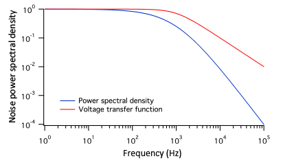
Figure 2. Noise spectrum example: transfer function and power spectral density of filtered white noise
An example with measured data
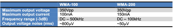
As a practical example, we show the noise characteristics and their interpretation for the Falco Systems WMA-100 (general purpose, low noise) and WMA-200 (ultra low noise) high voltage amplifiers (Fig 3). Their specifications are given in Table 1.
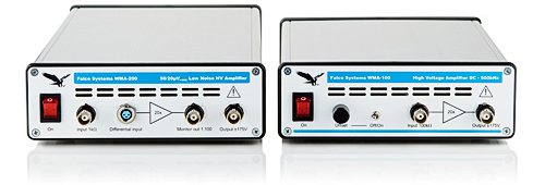
Figure 3. The WMA-200 ultra low noise and WMA-100 low noise (general purpose) amplifiers
Table 1. Specifications of the WMA-100 and WMA-200 high voltage amplifiers
The corresponding noise spectral densities and cumulative noise voltages versus frequency are given in Fig 4. The overall noise density per sqrt(Hz) of the WMA-200 is lower than that of the WMA-100 in the whole bandwidth, and in addition the amplitude starts to roll of at lower frequencies than the WMA-100 due to the smaller bandwidth of the WMA-200. Note that low-frequency interference components (50 Hz and other magnetic interference up to 10 kHz) are very visible in the power spectral density plots (Fig 4a), but that these contribute only a few microvolts to the total 50 uVrms output voltage noise of the WMA-200 (Fig 4b). The high frequency interference in the experiment (sharp peaks above 1 MHz in Fig 4a) is caused by radio signals, but its contribution to the cumulative total noise is negligible.
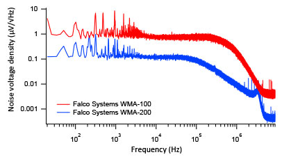
Figure 4a. Voltage noise spectral density
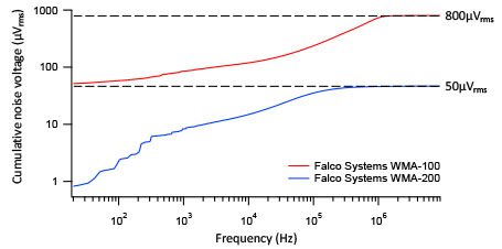
Figure 4b. Cumulative noise voltage
Figure 4. Experimental assessment of the output voltage noise spectral density and corresponding cumulative output noise voltage plot for the WMA-100 and WMA-200 high voltage amplifiers
Amplifier noise assessment pitfalls
Typical issues to watch out for are:
- The amplifier has a large bandwidth, but the manufacturer only quotes the noise level with a huge capacitive load, where the bandwidth is much smaller, but does not mention this bandwidth reduction.
- If the high voltage amplifier peaks with certain capacitive loads this may amplify noise frequencies at the peaking frequency enormously.
- Is there a lower frequency limit on the measured output noise? An oscilloscope on 'AC' to block a DC offset from influencing the measurements? A deliberate attempt not to show the 1/f noise? A wicked version of this error is to quote only the 'flat-band noise' with no graphs whatsoever.
- The amplification factor of the amplifier can be adjusted, but only the output noise for the lowest amplification factor is given.
- The noise has been measured (correctly) in a much larger bandwidth than the bandwidth of the amplifier, but the amplifier bandwidth is not mentioned. In this case you may be tempted to think that the output noise is spread over this much larger bandwidth, with a correspondingly lower estimated nV/sqrt(Hz).
- The noise is given in a bandwidth only up to the -3dB bandwidth of the amplifier, giving a value that is roughly 1.571 times lower than it actually is. This is a trap that even manufacturers may fall into in good faith, when plotting a cumulative noise spectrum up to the -3dB bandwidth of the amplifier instead of plotting it up to a frequency that is at least ten times higher.
- No low noise high voltage amplifier will help you if your signal source has too much noise...
Section 2 - Interference
Types of interference
Interference is not a random signal generated inside a measurement system due to the physical properties of that system itself. Instead, it is caused by outside sources of parasitic signals that somehow manage to get into the measurement system. Electrical interference can be coupled capacitively, magnetically, as a forced current in a common conductor, or by picking up high frequency electromagnetic radiation. Finding the source of non-electrical interference can be pretty easy if it is caused by e.g. thermal effects (slow drift), or vibrations and sound ('microphony' of the circuit). The latter can be identified (and countermeasures evaluated) by listening to your noise with headphones, a trick not everyone is aware of. An example of microphony that is not all that obvious is transformer hum that acoustically couples to a charged capacitor, causing 50/60 Hz currents. But non-electrical interference can be even more obtuse, as in the situation where cosmic radiation creates a leakage current (in short pulses!) through a high quality dielectric.
Capacitive interference
Capacitive interference typically forces its way into high-impedance (high resistance) nodes of a circuit that we use in a measurement setup. Essentially the metal of the high impedance node of the circuit and a conductor at the interference source act together as two plates of a capacitor with the air in between them as the dielectric. A changing voltage difference between the two can then cause a current to flow through this 'parasitic' capacitor, and end up at the high impedance node of the circuit. The higher the frequency of the voltage change at the source of the interference, the higher the current, and the more troublesome it becomes, as the impedance of the capacitor changes as 1/j*omega*C, with 2*pi*omega the frequency of the interference in Hz, and C the capacitance of the parasitic path in Farad. Typical capacitances are in the pF (10^-12) to fF (10^-15) range.
An example is a signal coupling in from the mains wiring in the walls (say 230 V rms, 50 Hz) to a little unshielded wire sticking out of a 1M-Ohm oscilloscope input. Many readers will have observed that this will cause a 50 Hz waveform to appear on the oscilloscope. It gets worse (higher amplitude) when one touches the wire with a finger. The situation and the equivalent schematic are given in Fig 5.
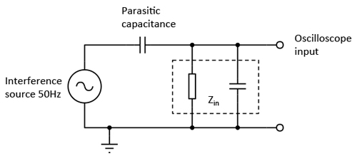
Figure 5. Capacitive interference at an oscilloscope input
The parasitic capacitance between the mains wiring and the oscilloscope input will form a high pass filter with the input resistance of the oscilloscope. The input capacitance of the oscilloscope (typically around 30pF) will cause graph of the rising interference signal at high frequencies to level off again. Using a value of a few pF of parasitic capacitance, and 1M-Ohm input resistance, the expected parasitic voltage at the input of the oscilloscope is easily calculated.
Many systems exhibit this type of interference and will pick up low frequency mains interference as in the example, or higher frequency interference such as radio waves in the MHz range. The latter may be outside the bandwidth of the circuit, but still cause problems if the parasitic signal is rectified by the pn-junctions of transistors or diodes in the circuit. It will then appear as a signal at a much lower frequency.
The countermeasures against such interference are essentially always the same: lower the parasitic capacitance between the source and the susceptible circuit node. This can be done by making the conductive area of the susceptible node of the circuit smaller, or by making the distance between the interfering source and the circuit larger. Both will lower the parasitic capacitance. But by far the most effective is to place a third, grounded, shielding conductor between the two nodes such that the susceptible node cannot 'see' the interfering node anymore (Fig 6).
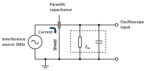
Figure 6. Shielding a sensitive high-impedance node against capacitive interference
With such a conductive shield, the interfering capacitive current will be conducted to ground before it can do any harm. When this shielding conductor is placed all around the susceptible circuit, we speak of a Faraday cage. It can take the form of a small box on a PCB or a conductive, grounded enclosure (as in most low noise high voltage amplifiers). But even complete rooms can be shielded, as is the case e.g. in EEG (electro-encephalogram) measurement rooms in hospitals. Another example is shielded cable such as coaxial cable, but we will have to say more about cabling later. At low to medium frequencies (up to the MHz range) this shielding can be remarkably effective, with 120dB (a factor 106) reduction in interference being not unheard of.
In conclusion: to prevent capacitive interference, reduce the parasitic capacitance as much as possible and employ a grounded shield, preferably all around the susceptible node, so that the shield effectively becomes a Faraday cage.
Magnetic interference
Magnetic interference is basically 'transformer action'. It will occur if there is a conductive loop in which changing magnetic field from the surroundings can induce a current. As this current revolves around the loop, it will create voltages across every significant resistance and impedance present in the loop. The loop is not necessarily a physically discernible loop: the loop current can e.g. pass through (parasitic) capacitances, which makes it sometimes difficult to see where the interference is coming from.
The ground loop is a well-known type of magnetic interference (Fig. 7). Here, the 0 Volt ground reference is not everywhere at the same potential, because the induced circulating current will create voltages across the resistance of the loop. A large loop area is especially detrimental, because a lot of magnetic flux will be able to pass through it. A typical example is two pieces of equipment that are both grounded to the mains protective earth, but which also communicate with one another using a single ended cable such as shielded coax. Here low-level measurements will pick up magnetic interference via the typically large area of the loop of the protective earth wires (in the mains cable) and the coax.
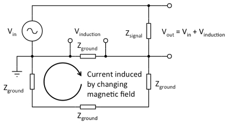
Figure 7. A current induced by a changing magnetic field flux in a 'ground loop' will cause voltages to appear along the loop because the current flows through a non-zero resistance/impedance.
The most important countermeasures against magnetic interference are increasing the distance to the interference source, and making the loop that picks up the magnetic interference as small as possible.
Contrary to capacitive interference, which can be completely solved by a conductive enclosure, magnetic interference is much harder to shield. The reason is that there is no perfect magnetic material. Steel (not stainless - most stainless steels are non-magnetic) will work reasonable well, and, for difficult cases, mu-metal is an option. However, mu-metal is expensive, and difficult to machine, because under stress (e.g. bending) it will loose it excellent magnetic properties.
Just placing a piece of magnetic material between the offending source and the receptive loop will not work, as the magnetic field lines will just go to the shielding piece, and then further to the receptive circuit. Instead, one needs to duct the magnetic fields around the susceptible circuit (Fig. 8).
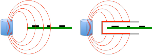
Figure 8. To shield against magnetic fields, one has to guide the field lines around the susceptible circuit with magnetic material.
Forced currents
If a current flows between two ground points that are supposed to be at the same potential, this common 0V reference does not work anymore, because the current will induce a voltage across any resistance it encounters between these two points. An example is where a sensitive circuit sees different ground potentials at different places due to a large current flowing from the power supply to a power circuit that draws its current through the sensitive circuitry. The solution is to provide a separate conductor to the power circuit for every connection through which significant currents are expected to flow.
'Star grounding' of the sensitive circuit helps here as well, where all the 0V nodes of the sensitive circuit are tied together in a single point. Even if there is current flowing through this point, the resistance between the different ground connections is negligible because they are not separated in space anymore. Therefore there will be no voltage differences between the ground points of the sensitive circuit. But often a low-impedance ground plane on the printed circuit board (PCB) is an even better solution.
Electromagnetic radiation
At high frequencies, the physical length of the electromagnetic waves becomes comparable to or smaller than the physical dimensions of the measurement system. In this case the simplification of separate capacitive and magnetic interference does not hold anymore. The wavelength lambda in meter is related to the signal frequency f in Hz as lambda = nu/f , with nu the speed of light, 3*10^8 m/s. A rule of thumb is that for frequencies where the wavelength is smaller than 10x the largest dimension of your system, you will have to take electromagnetic effects into account. But for a highly sensitive circuit, you will already experience the effects at much lower frequencies.
Fortunately, shielding with a Faraday cage typically works very well against electromagnetic interference. The electromagnetic radiation will create eddy currents in the shield that will, if the shield has a sufficiently low resistance, completely cancel the electromagnetic radiation on the other side of the shield. Radio reception is a well-constructed Faraday cage is completely impossible! If holes in the Faraday enclosure are required, they should be small compared to the length of the electromagnetic wave that you try to keep out.
Enclosures and cabling
A metal enclosure that conducts across all surfaces is a very good general-purpose Faraday cage. A coaxial cable between two enclosures will also act as such (Fig. 9). This scheme will give excellent interference rejection performance. If the enclosure does not conduct well across all surfaces and interfaces (notably if the enclosure consist of different panels screwed together), the effectiveness of the shielding is impaired, and an experimental assessment of the interference levels inside the enclosure may be necessary.
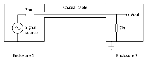
Figure 9. Two enclosures with a coaxial cable between them act as a single Faraday cage. The circuitry inside will not be disturbed by capacitive or electromagnetic interference.
Unfortunately, most often there are more cables present than in the scheme of Fig. 9. This introduces the risk of ground loops and the pickup of magnetic interference. Keeping the cables as short as possible and the area of the ground loop minimal will help somewhat, but the best solution is to use a differential signal between pieces of equipment. Some function generators have two outputs to accomplish this task, and ultra-low noise high voltage amplifiers have a differential input to reject the interference caused by the processes described above.
A single ended signal has a fixed 0V reference, typically the shield. This is the way a coaxial cable functions. In the differential scheme, the source sends out two voltages on two signal wires. These wires carry a signal voltage of opposite polarity with respect to one another. The grounded shield can now pick up any parasitic voltage from the surroundings, but this will not influence the voltage difference between the two signal wires. This voltage difference is used at the receiving end, and hence there is no interference introduced.
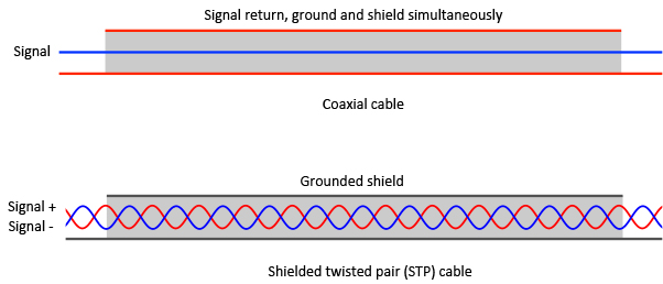
Figure 10. Both a coax and a shielded twisted pair (STP) cable pick are built such that their symmetric geometry that currents induced by a changing uniform magnetic field in one loop will be cancelled in another loop. In addition to magnetic interference cancelling, the STP cable will also shield against voltages generated in the shield by ground currents, which the coax cable does not.
A differentially connected system may still be somewhat susceptible to magnetic interference. There exists a loop between the two signal wires because they are not exactly in the same spot. Twisting the wires will reverse the influence of a changing magnetic field at every twist. The small magnetic interference picked up by a small loop section of the wire will be cancelled by the next loop, where the magnetic interference is induced with the opposite polarity. This is the principle behind the twisted pair cable (Fig 10).
Recommendations for high voltage amplifiers
High voltage amplifiers are not unique in their susceptibility to external interference, and all recommendations above apply. Specifically the following should be noted:
- Use a differential signal and an STP cable between the signal source and the high voltage amplifier if possible.
- If a single ended (coaxial) cable between the signal source and high voltage amplifier is needed, keep the coax cable as short as possible. A ground loop may exist between the signal generator and the high voltage amplifier, because both are often connected to the mains protective earth through their mains cables. Some generators have an independent signal ground, or offer the possibility to disconnect this ground from the mains safety ground if required, thereby preventing a direct ground loop. Other signal generators can run on batteries. A capacitively coupled loop of lesser severity may still exist. Use short mains cables, connect them to the same outlet, and tie them together along their length as far as possible.
- The output of a typical high voltage amplifier is single-ended, unless two amplifiers are used in bridge mode, and is hence susceptible to all the external influences listed above. Use the amplifier output connector ground to ground the load of the high voltage amplifier, e.g. the piezo, MEMS, etc. If one would make a separate connection from the load to another ground point, a ground loop would be created instantly, and the voltage accuracy across the load will be impaired. Keep the connecting single-ended coax cable from the amplifier to the load as short as possible: on the uV level, centimeters are even better than decimeters!
- Shield the load with a Faraday-like enclosure if at all possible, and ground this enclosure to the ground of the output of the high voltage amplifier only.
Fig. 11 shows the recommended ways to connect generator, high voltage amplifier and load for optimal interference rejection. Fully differential operation is not always possible, especially on the load side in which case one is left with a non-optimal solution, where some interference will always be present. However, by heeding the advice given above on minimizing interference (short cables, minimizing loop area, shielding high-impedance nodes, etc., often a workable compromise can be obtained. One can also consider using two high voltage amplifiers and driving the load itself differentially, also called 'bridge mode'. The added advantage is a doubling of the peak-to-peak voltage compared to what is possible with a single high voltage amplifier.
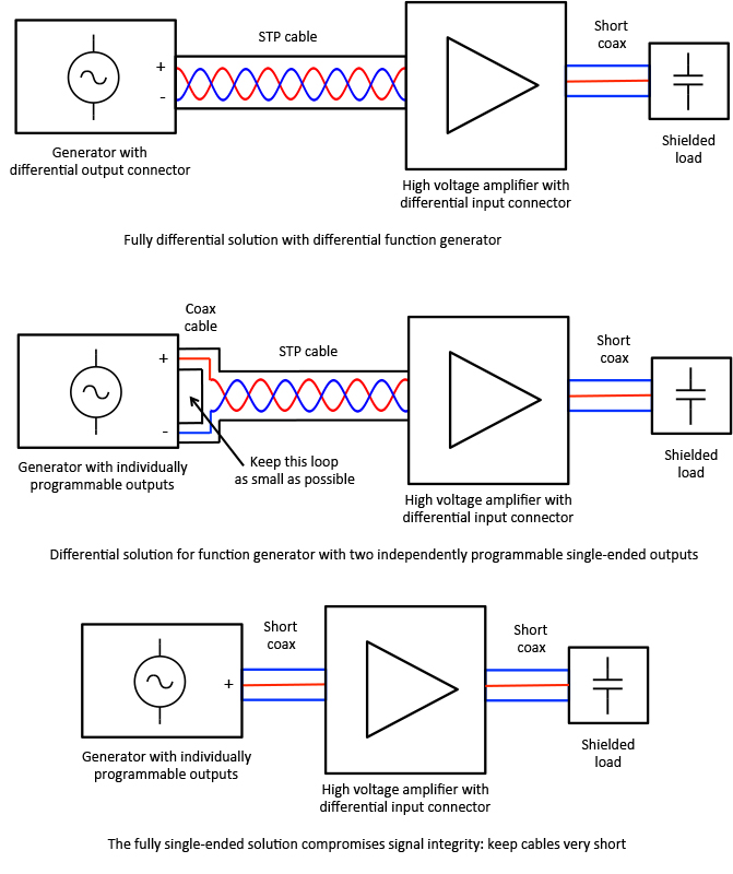
Figure 11. Recommended ways to connect generator, high voltage amplifier and load in the presence of external interference
References
[1] C. D. Mothenbacher and J. A. Conelly, Low-noise electronic system design, Wiley, New York, 1993