Driving piezoelectric actuators with high voltage amplifiers
PART I - Piezo materials, applications, precision, speed, and damping of resonances
Falco Systems application note, version 1.0, May 2018
W. Merlijn van Spengen, PhD, vspengen@falco-systems.com
Introduction
Piezoelectric crystal actuators (piezo's in short) are used in many applications, because they pair a high stiffness, force, and maximum operating frequency with a very high positioning resolution.
In this application note, many piezo-related topics are introduced and discussed briefly. We cover the basic piezoelectric effect, the hysteresis of piezo's, and how different types of piezo actuators are constructed. The application possibilities of piezo's are almost endless, and a number of examples are presented, such as scanning probe microscope scanners, stick-slip motors, and piezoelectric transformers. Because piezo's are often used in precision positioning systems, the next section covers the decoupling and damping of external vibrations. The importance of a small mechanical loop is explained, and examples are given of vibration isolation solutions. The options to reduce vibrations coupled into the mechanical system by the piezo itself are also addressed.
Then we focus on how to drive piezo's with high voltage amplifiers. Because this is common in the field, we will use 'piezo driver' in this application note, instead of the more general term 'high voltage amplifier', while noting that these describe basically the same equipment. Falco Systems offers a wide range of high voltage amplifiers (high speed/low noise/battery powered), many of which are used extensively as piezo drivers all over the world. Using a high-quality driver, piezo positioners can have exceptionally high positioning resolution and repeatability, although the absolute accuracy is poor due to hysteresis. This hysteresis can be reduced (but for high frequencies not entirely eliminated) by negative feedback using a position sensor signal, and by charge control. High-speed actuation of piezo's requires the quick charging and discharging of the large piezo capacitance. The maximum current of the piezo driver limits the slew rate and hence the attainable maximum speed.
In the last section of this application note recommendations are given for choosing a network to connect a piezo to its driver, which maximizes bandwidth and minimizes the influence of the piezo resonances. Part II of this application note (a separate document) contains the in-depth discussion of such coupling networks and the optimization of the piezo response.
It is hoped that we can help many readers by presenting this information here, which is partially based on the authors' previous experience at IMEC, Leiden University, the TU Delft and in different projects and user committees. Please feel free to contact the author if you have questions related to the topics covered in this application note.
Piezoelectric materials
Piezoelectric crystals share the physical property that they will generate an electric field when deformed (the direct piezoelectric effect), while they will also deform in an applied electric field (the converse electric effect). This is possible because these crystals have a spatial distribution of the internal charge that changes under deformation. A good example of a piezoelectric material is the common lead zirconate titanate (PZT). While the electronics industry has converted to almost completely lead-free solder manufacturing, high-quality lead-free PZT-material equivalents are not available yet, despite extensive research.
In Fig. 1 the lattice of a PZT crystal is shown, with the charged atoms indicated. Above the Curie temperature, the positively charged Zi or Ti atom fits in the middle of the crystal unit cell, and no dipole is present in the crystal. Below the Curie temperature the lattice shape changes and the large, positively charged atom no longer fits in the middle of the unit cell. The positively charged atom finds a new equilibrium position off-center, a dipole is created, and a net polarization of the material results. When the piezoelectric material below the Curie temperature is strained, the length of the dipoles in the unit cells will change, which gives rise to the piezoelectric effect.
Figure 1. The PZT crystal unit cell has a dipole when the material is below the Curie temperature
In some piezoelectric materials, all the dipoles are oriented in the same direction, such as in naturally occurring quartz. Stronger, synthetic, polycrystalline piezoelectric materials such as PZT have their dipoles oriented in the same direction only in small Weiss domains, similar to the situation in magnetic materials. Due to the random orientation of the Weiss domains, these materials have no intrinsic net piezoelectricity. By applying a high external electric field while the crystal is above the Curie temperature, and then slowly cooling it down to below the Curie temperature, these domains can be 'lined up', and a strong remnant polarization is induced. The electric field can usually be applied to a piezo by connecting a voltage source to electrodes glued onto both sides of the piezoelectric crystal. These electrodes can subsequently be used for sensing (direct piezoelectric effect) or actuation (converse piezoelectric effect), see Fig. 2. Many piezo's will partially depolarize when the electric field is reversed compared to the direction of the field with which it was polarized. This gives rise to increased hysteresis and permanently lowered gain. Unipolar actuation with voltages of the right polarity (or at most around 20% of the maximum voltage in the reverse direction) is recommended for driving most piezo's, and the actuation leads are marked accordingly.
Figure 2. Sensing and actuation with a piezoelectric crystal
The piezoelectric effect is a combination of mechanical and electrical properties of a material in all directions, giving rise to a number of defining anisotropic vector equations and property matrices. Because often only one electrical and one mechanical axis are important, we can simplify these vector equations and property matrices into one-dimensional approximations. Both the direct and converse piezoelectric effect can be captured in such a single set of equations [1]
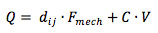
Here, delta is the elongation (strain, displacement) along the force axis, F_mech is the force applied (direct) or generated (converse), k_piezo is the stiffness (spring constant) of the piezo, and V is the voltage generated (direct) or applied by a piezo driver (converse) at the plates on the opposite sides of the crystal. C is the capacitance between the plates, and Q the charge accumulating on them. The polarization direction of the piezo can be different depending on the application of the crystal, e.g. for a linear mode or shear piezo. The piezoelectric coefficient d_ij relates the strength of the piezoelectric effect (the 'gain') with magnitude d between the polarization direction i and the displacement direction j. The maximum displacement of a piezo is usually around 0.1% of its total length.
Piezo's are very 'strong' actuators, i.e. they have a high stiffness. The force available that a piezo can exert to its surroundings can be calculated as follows. If the piezo is unconstrained at one end, this free end will displace an amount delta to a force F as linked by its internal stiffness k_piezo as

If the piezo is clamped on both sides by an infinitely stiff support, the displacement will be zero, and the same force F is available to press against the support, so the maximum 'blocking force' F_max that a piezo can exert (or withstand) at zero displacement is also equal to k_piezo*delta. Note that here F_max is the maximum force available in the case the piezo is completely constrained, which relates to the displacement delta of the same piezo in the unconstrained case. F_max as given here is a small signal property: for large displacements F_max is usually smaller, up to a factor two, due to polarization changes in the material.
The equations above promise infinite positioning resolution (smallest discernable change in position) and accuracy (known, repeatable 'correctness' of the position). The attainable positioning resolution of piezo's is indeed exceptionally good. Unfortunately, piezo actuators and sensors suffer from significant hysteresis and creep, affecting the positioning accuracy. Creep manifests itself as the fact that the displacement of a piezo is not the same on the positive and the negative going part of an actuation waveform. The Weiss domains have a distribution in how well they align with the electric field at different actuation voltages. But once aligned, they will only return to their previous state at a lower voltage that needed for them to do the alignment in the first place, due to molecular friction. As a result, the piezo carries some memory of what has happened to it before. The hysteresis in the displacement between the increasing and decreasing voltage curve (and hence the accuracy) is typically a few percent of the total displacement. Creep is the change in displacement over time while keeping the actuation voltage from the piezo driver constant. It is caused by the same changes in the material that are also responsible for hysteresis. The rate of creep typically diminishes logarithmically as a function of the time that the voltage has been constant.
If we recall the equation for the charge on the plates
we see that the voltage is related to the mechanical force (and hence the displacement via k_piezo) via the piezo capacitance. The piezo capacitance C is

in which epsilon_0 is the dielectric permittivity of free space, epsilon_r is the relative permittivity of the piezo dielectric, A the total area of the actuation plates, and d the separation between these plates. It is via epsilon_r that the piezo polarization changes (and hence hysteresis) enter the equation. If the piezo is driven by a charge instead of a voltage, there is a direct relation between this charge Q and F_mech. Indeed, if driven by a charge control piezo driver instead of the common voltage piezo driver, most of the hysteresis of a piezo disappears [2]. Charge control is discussed in more detail later in this application note. The difference in hysteresis between voltage control and charge control is shown in Fig. 3.
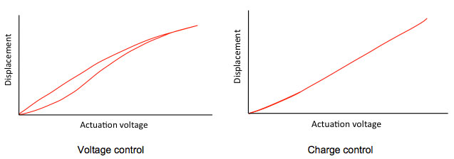
Figure 3. Piezo's exhibit hysteresis when driven by a voltage control piezo driver, but much less so if the charge on the plates is the controlled parameter, redrawn from [2]
Piezo's are brittle ceramics or single crystals, and hence fairly fragile. While they can stand a high compressive force, they are vulnerable under tension and bending conditions. Because of their high speed and force capability, care has to be taken that a fast accelerating/decelerating mass driven by the piezo (either its own mass or something that it is displacing) does not damage the piezo. An effective moving mass m changing its speed with an acceleration a exerts an inertial force F = ma on the piezo, and if this force is in the elongation direction, it should be kept smaller than the maximum tensile force given by the manufacturer. Do not drive your piezo with electrical signals that are too fast! Calculate the effective mass of your assembly and the maximum acceleration if in doubt.
To prevent tensional loading, piezo's are often pre-clamped at the moving end, using a flexure spring that sets the piezo under a compressive force when it is not actuated.
Piezoelectric actuators and applications
Well-known companies supplying piezoelectric actuators are e.g. Physik Instrumente and Noliac, but there are many others. Depending on the size, thickness, polarization direction and the locations of the electrodes, piezo actuators can be classified in five broad categories: linear mode, shear mode, tube, bending mode, and MEMS (micro-electromechanical systems), see Fig. 4. Of course, many variations are possible, as piezo actuators can be produced in almost any shape. A linear mode piezo actuator can e.g. be a cube, rod, plate, disk or ring, and a tube scanner can e.g. be either a cylinder or a cone shaped actuator, the latter having a lower effective moving mass and hence a higher resonance and operating frequency than a cylindrical tube.
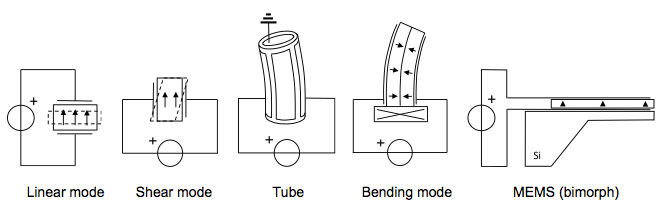
Figure 4. Common classes of piezo actuators
Piezo actuators need fairly high electric fields to operate. To make the corresponding drive voltages more manageable, usually the piezo is built up from thin slices of piezo material with the electrodes interdigitated between them (Fig. 5), as a so-called stack piezo. In the way depicted, the actuator slices are mechanically in series and electrically in parallel. This decreases the operating voltage, e.g. from 1000V to 100V, but also increases the piezo capacitance. While this takes away one drive problem, it may create another at high speeds, because large currents are required to charge and discharge this larger capacitance of a stack piezo fast enough.
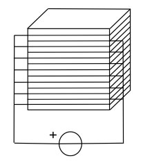
Figure 5. Stack piezoelectric actuator (the polarization direction changes from up to down and back to up from layer to layer)
In a linear mode piezo, the polarization is in the same direction as the displacement. The corresponding piezoelectric coefficient given by the manufacturer is d_33. The displacement is a simple elongation of the crystal in the direction of the applied electric field. These are the most commonly used piezo's. Depending on how many plates are used in the stack (if any stack at all is used), and the size, the maximum displacement can range from less than 100nm to over 1mm.
Linear mode piezo's find application from high-speed precise position stages for e.g. scanning probe microscopy (SPM) to damping vibrations in buildings. Another well-known application is e.g. in active vibration isolation, in which externally coupled vibrations are actively compensated by the motion of one or more piezo's in the opposite direction. In a scanning acoustic microscope (SAM), very high frequency (MHz range) acoustic signals are sent out by a linear mode piezo, and used to create an image of an object under study. Contrary to optical microscopy, the internal structure of the object can be seen in a SAM, because high frequency sound waves will penetrate the object, and will be reflected at the interfaces between different material densities. Its working principle is very similar to very small-scale sonar. A personal favorite of the author is the Physik Instrumente PIFOC range of products, where a piezo stack is used to focus the objective of an optical microscope [3], which can be used to build excellent autofocus systems. But the mundane piezo 'loudspeakers' of children's toys and the high-quality under-the-bridge 'bar' pick-up sensors of amplified acoustic guitars (the latter is another of the authors' favorites) are linear mode piezo's too: the possibilities of linear mode piezo's are almost endless.
In shear mode piezo's, the polarization direction and the electric field are under a right angle, and when actuated, the piezo shears sideways. The corresponding functional piezoelectric coefficient here is usually d_15. Shear mode piezo's find use in compact scanners, and in stick-slip motors. In the latter, also called piezoelectric inertia motors, a shear piezo carrying a mass (its own mass, or e.g. a positioning stage) rest on guiding rails or just a flat surface, but is not fixed to it. A second way to design such a motor is to use a linear mode piezo, with two masses. Both types are indicated in Fig. 6. The piezo is slowly deformed by the actuation voltage, and the mass it carries moves with it. Due to the friction between the slider and the surface on which it rests, the contact between the piezo and the surface is kept, and the result is a net displacement of the center of mass. Then the piezo is suddenly brought back to the original shape by a 'step' voltage change from the piezo driver. Because the mass cannot follow instantaneously, the whole moving assembly, including the piezo, will keep its center of mass position. The piezo or contacting mass will for a very short time 'slip' along the surface on which it rests, and a net displacement results. By applying a sawtooth-shaped voltage wave to the piezo, the stick-slip motor can be made to 'walk' over the surface or in the guiding rails.
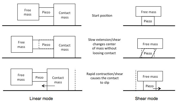
(a) Principle
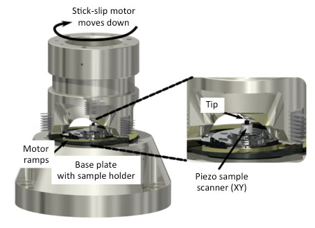
(b) STM (scanning tunneling microscope) coarse approach head design with a three shear piezo stick-slip motors on a curved ramp
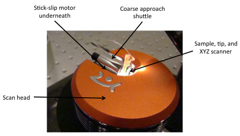
(c) The shuttle of the Nanosurf Easyscan STM [4] is also moved with a stick-slip motor
Figure 6. Piezo stick-slip motors; examples adapted from [5]
The company Attocube has a nice range of scanners based on the stick-slip motor principle, and Nanosurf uses a stick-slip motor to bring the tip of their entry-level scanning tunneling microscope (STM) in small steps in contact with the object under study ('coarse approach'). Compared to other piezo-based positioning stages, the stick-slip motor has the advantage of a virtually unlimited range: the minimum step size is governed by the electrical and mechanical dynamics, and the maximum displacement only by the length of the guiding rails on which the piezo moves. The stick-slip contact should be kept clean and dust-free for the motor to operate properly.
Tube scanners consist of two X and Y electrode pairs at 90 degree angles of each other on shear mode piezo tube body, and often contain a Z-direction electrode pair as well. The counter-electrode is a common, grounded metallization on the inside of the tube. The electrode pair is driven differentially, that is, one electrode receives a positive actuation voltage from the piezo driver, and the other one on the opposite side a negative actuation voltage of the same magnitude, with a common ground on the inside of the tube. Tube scanners can be used to make a two-directional XY scanning motion in a single, space-efficient actuator with a large stroke. Actually, the motion is following the top of a large radius sphere; if necessary, corrections can be made in the z-direction with a separate Z-scanner. Usually a Z-scanner is integrated with the XY scanner. In this case there is an extension of the tube where there is one outer and one inner and electrode completely covering the circumference of the tube scanner. Applying a voltage between these two Z-electrodes will elongate the tube. Alternatively, the X and Y electrodes can be actuated simultaneously with respect to the inner tube electrode to create a displacement in Z, although this complicates the drive signal (Fig. 7).
Bending mode piezo's are typically flat, one-side fixed thin plates or beams with top and bottom electrodes, and the piezo consists of two pieces of material polarized in the opposite direction with respect to one another (see Fig. 5). Normally only small displacements are possible between the electrodes of a piezo actuator. But in this case, when in resonance, due to the mechanical amplification by the long beam, large displacements (larger than the thickness of the plate) can be obtained at the far end.
Piezoelectric transformers are based on this principle (Fig. 8). These have two large electrodes with a large capacitance between them near the fixed end of the beam to set the piezo in motion. The large resonant displacement amplitude at the free end creates a high voltage at the (smaller) plate at the free end. Just like in a magnetic transformer, the higher voltage side has a smaller current drive capability: no net energy is being generated. The energy is only transferred from one side of the beam to the other, basically acoustically.
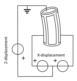
Figure 7. XYZ piezo tube actuator
Figure 8. Piezo transformer operating principle. Due to the large deflections,
a high output voltage is generated on the right hand side
The piezo transformer only operates correctly if it is driven at its resonance frequency. This resonance can change with temperature, aging, and electrical loading conditions (this actually holds for all piezo's). Hence fairly elaborate driving and control circuits are required to keep the input drive signal voltage appropriate for the momentary condition of the piezo [6]. Piezo transformers were once popular for generating the high voltage for backlights in LCD notebook computer screens, but have now been superseded by other display technologies. Testimony to this is the obsolescence of the dedicated driver chips that were once offered in large quantities at low prices, but are now almost unavailable. However, micromachined MEMS piezoelectric transformers could potentially be used as highly miniaturized high voltage generators on a chip, and they are a recent, active field of research [7].
In MEMS technology, piezoelectric actuators are often used as actuators, and not only for free-standing structures. They are often used to launch acoustic signals into mechanical filters such as surface and bulk acoustic resonators. They are also used to create (test) displacements for acceleration sensors and gyroscopes. Furthermore, piezoelectric layers are used extensively in MEMS for sensing purposes. MEMSCAP offers a multiuser process called PiezoMUMPS, where experimental MEMS structures including a piezoelectric layer can be manufactured at relatively low cost [8].
External and piezo vibration damping
The intrinsic material properties of a piezo determine to a large extent the mechanical response of a piezoelectric actuator. A piezo is a resonant system with a low damping factor, so low in fact that, if optimized for this purpose, the high-Q piezo resonance can be used in watches and frequency standards for timekeeping.
The stiffness of the piezo is highly appreciated for actuation purposes, but usually its resonance is not, except for alarms and certain types of ultrasonic transducers. Even when the piezo is not actuated, the resonance can be seen by the 'amplification' of vibrations coupled into the system from the outside world. In Fig. 9, a simple model of a positioning system is depicted. This model describes a large range of cases, from an optical table measurement setup to scanning probe microscopy (SPM, e.g. AFM (atomic force microscopy) or STM (scanning tunneling microscopy)). The common property is that they all have a point that has to be actuated with high precision (the 'actuator position') relative to some object reference position (the 'object position').
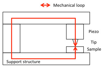
Figure 9. Keep the mechanical loop small and stiff
The stiffer the total mechanical loop, the less the loop deforms when subjected to an external force, and the better the position accuracy of the actuator position relative to the object position. A small loop is typically stiffer than a long loop, because, all other parameters held equal, a beam twice as long will have an out of plane bending stiffness eight times smaller, and a compressive stiffness two times smaller. Therefore, precision positioning systems are often designed to be mechanically as compact as possible, at least with respect to the loop along the path from actuator to object.
The next step is to decouple the loop from outside vibrations. In Fig. 10, three 'advanced' versions of commonly used solutions are shown. In optics, this is usually done with an 'optical table', a heavy mass table with no own resonances on legs with springs. The table itself is often a stone (granite looks nice and can be machined to be very flat). If many mounting holes are required (an experimental 'breadboard'), metal tables can be used as well, but they are constructed in specific ways to prevent resonances in the table bed. An example is Newport, a large optics manufacturer and distributor, who has a dedicated 'honeycomb' structure inside their metal optical tables [9]. The AFM community, in need of sub-nm stability of the mechanical loop, takes a similar approach. The AFM itself, a small apparatus with an even smaller mechanical loop, is placed on a small, heavy mass table, and suspended in bungee cords (the damped springs) inside a sound-proof box, with doors for easy access to the AFM. Sometimes this box is placed on an optical table again, for even more isolation from ground-conducted vibrations. STM experiments (with sub 100-pm resolution) are usually performed in UHV (ultra-high vacuum), and large vacuum chambers are required. These can be suspended on legs with springs, in the same way optical tables (and cars) are. Inside the vacuum chamber, the platform containing the STM is suspended in the same way as for AFMs. Because the use of most materials in a UHV is out of the question due to outgassing, the bungee cords are replaced by metal springs. As these springs have no damping, this is accomplished by mounting magnets on the vessel side, and copper plates on the platform, or the other way round. If the magnets move relative to the copper plates due to vibrations coupling in, the vibrations will be damped by the dissipation of the eddy currents that are induced in the copper by the moving magnets.
All these approaches boil down to the same basic principle: decouple the system from its surroundings by a low frequency mass-spring system, and add damping until the vibration isolation system (ideally) behaves as a critically damped second order system. Fig. 11 shows the tradeoffs involved. A first order system will have no resonance, but does not decouple really well at high frequencies, as it has a '-1' slope (10 times amplitude reduction per decade of frequency). Having a '-2' slope (100 times smaller amplitude per decade), a resonant second order system has good damping at high frequencies, but has a high coupling amplitude at the resonance frequency. An overdamped second order system has the same -1 slope as the first order system until at some much higher frequency than the -3dB cut-off frequency the second order behavior takes over. The ideal, then, is to create a vibration isolation system that behaves as a critically damped second order system with as low a cut-off frequency as possible, and critical damping, because the frequency response will then fall off with a -2 slope immediately above the cut-off. Some optical tables also employ 'tuned damping' to bring down the underdamped second order resonance peak.
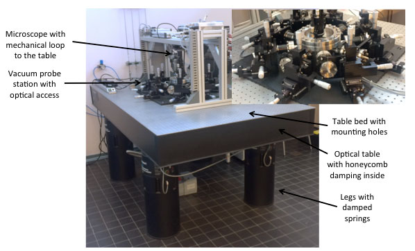
(a) Optical tables have damped springs in/on the legs and come in many shapes: this table has a large hole in the middle and a vacuum probe station mounted on it: the molecular turbopump is on the bottom side, suspended under the optical table. It is used in [10]
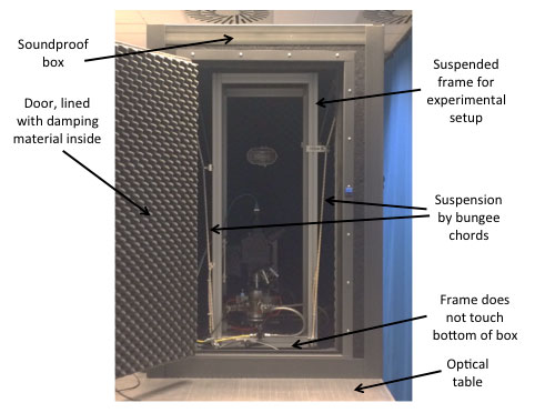
(b) Vibration isolation stage with microscope in soundproof box, damping is in the suspension bungee cords, as used e.g. in [11]. This concept is also often also used for AFM
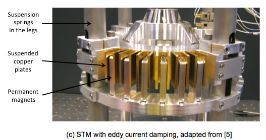
(c) STM with eddy current damping, adapted from [5]
Figure 10. Vibration isolation examples with damping
In actively damped vibration isolation systems such a response is often easier to obtain than with only passive masses, springs and dampers. The disadvantage of an active vibration isolation stage is that it will more easily generate large overshoots or even oscillations if loaded with the wrong mass or if the center of mass is not at the 'right' position that the control electronics expects. Active vibration isolation can be recommended for permanent setups, but not so much for experimental ones, where things change all the time. Active systems do have more possibilities for 'perfect' vibration isolation, though. One example is e.g. 'skyhook' damping, where the absolute velocity of the stage is measured relative to a suspended stationary 'seismic' mass and actively counteracted. The result is (ideally) no transmission of vibrations at all, up to very low frequencies, as if the stage was 'hooked to the sky' [1].
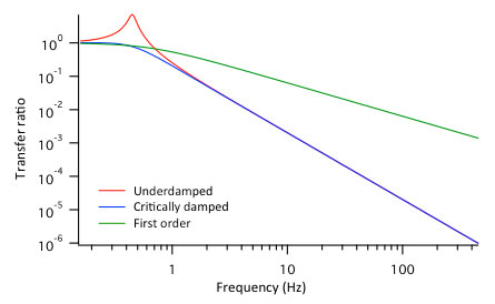
Figure 11. Good vibration isolation is obtained by a critically damped second order system with a low cut-off frequency
Passive piezo-based vibration isolation and compensation is also used [12]. In this case the piezo is connected electrically to a damping network that matches the transfer function of the piezo. This is done using one or more resonant circuits with damping, created with an inductor and a resistor, the capacitance of the electronically resonant circuit being formed by the piezo capacitance itself. Because often the inductance required is rather large, it is also an option to replace the inductor by an electronic inductance-simulating equivalent, using a gyrator active circuit. Electronic piezo-matching circuits are discussed extensively Part II of this application note in the context of optimal piezo actuator coupling circuits (see also the last section).
The piezo actuator itself has a very high quality factor Q, with sharp resonance peaks. In addition to 'amplifying' vibrations from the outside world, it will also resonate will large amplitude if its electrical drive signal contains any power at its resonance frequency. Being determined by material properties, it is not straightforward to mechanically filter these vibrations out, though damping material such as stone/concrete or rubber (or even the glue with which the piezo is mounted in place) in the mechanical loop can be beneficial, especially if used on both sides of the piezo.
To prevent the motion of the piezo actuator from setting up resonances in the mechanical loop, a complementary approach is to keep the center of mass of the actuation stationary, by adding a 'counter-piezo', Fig. 12. The counter-piezo is of the same type as the actuation piezo, but driven such that it moves in the opposite direction. In this way, it compensates for the vibrations that are launched into the mechanical loop by the actuation piezo by destructive acoustic interference. At low frequencies, this works fairly well (up to the precision with which the piezo's are equal). Due to the sharp resonances of the piezo's, of which the frequencies are almost never exactly equal, the beneficial effect often reduces as the actuation frequency approaches resonance. Also, it is difficult to cancel torsional forces on the support structure this way.
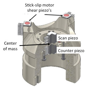
Figure 12. The center of mass is kept stationary with respect to the mechanical loop by using a counter-piezo, example adapted from [5]
Steering the actuator with a piezo driver: resolution, accuracy, speed and power
The positioning resolution of piezo's can be excellent. If state of the art piezo drivers are used, such as the ultra low noise Falco Systems WMA-200 high amplifier, the electronic contribution to the noise can be almost negligible. If the WMA-200 model is used as a unipolar piezo driver with 0 – 175V output voltage range and 50uV_rms noise in DC - 100kHz, the electronic resolution is 50*10^-6/175 = 2.7*10^-7 times the full scale displacement. If the piezo has e.g. a 10um range, this corresponds to a resolution of 2.7 pm_rms, independent of the actuation voltage. Of course, the signal generator steering the piezo driver should have a matching low noise performance. In practice the resolution can be larger than this, e.g. if the piezo exhibits friction against a flexure hinge. For the highest resolution applications, the piezo should be free to move independently.
Electrostatically actuated MEMS (micro-electromechanical systems) rival piezo actuators in their precision and accuracy. These are microscopic moving structures that can also displace on the order of a few microns. If properly designed, they can have much lower (or even no) hysteresis, but they have a very low stiffness compared to piezo's, typically on the order of 1N/m. Resonance frequencies of MEMS can be very high, even higher than those of typical piezo actuators. It is however interesting to note that the resulting position noise of a piezo caused by the piezo driver is typically lower than that of a comparable MEMS device. To first order, a piezo reacts linear to the actuation voltage of the piezo driver. The intended actuation signal and the noise voltage are superimposed on each other. The position noise at low or high actuation voltages is equal. Electrostatic MEMS devices react to the square of the actuation voltage. The result is that a noise term where the noise is multiplied by the momentary actuation voltage dominates the position noise at high actuation voltages. This term is typically larger than the noise term for piezo actuators. A comprehensive application note "The electrostatic actuation of MEMS with high voltage amplifiers: from comb drive levitation and pull-in to dielectric charging and position noise" is available here for more information.
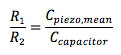
Although hysteresis limits the accuracy of the piezo to often no better than a few percent under large signal conditions, a periodic scanning motion with constant amplitude can have a very high repeatability, as long as the position used is always on the same side of the hysteresis curve (Fig. 3). This is the reason that AFMs and STMs can have a very high in-plane precision without resorting to position correction using a control loop. The hysteresis can be considerably reduced if a charge control scheme is used, as discussed above in the piezo material section. A common implementation is given in Fig. 13 [13]. The output voltage coming from the piezo driver is fed to a capacitive voltage divider consisting of the piezo actuator and a high quality capacitor.
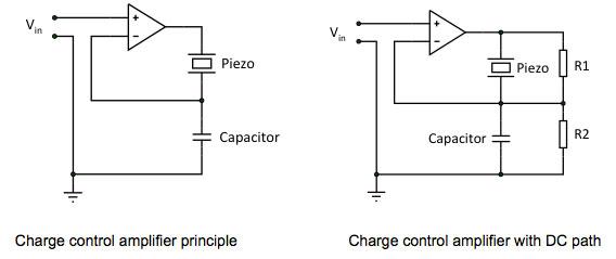
Figure 13. Reducing hysteresis of piezo actuators with charge control
The configuration with only capacitor and piezo is not stable at low frequencies, where the impedances of the capacitances go to infinity. To prevent the situation where leakage currents let the amplifier drift and make it clip to the power supply rails, a DC path consisting of two resistors is used to define the voltage across the piezo at very low frequencies. A frequency-independent response will be obtained if
Sometimes the resistors are replaced by a more complex current source scheme [14]. Although charge drive works, it is relatively little used. The complexity of the setup is larger, the system contains a control loop that is potentially unstable, and if multiple channels are used with a single counter-electrode, e.g. with tube scanners, the issues related to cross-talk between the channels are almost insurmountable. In addition, the resistors for the DC path are necessarily high-valued types, typically in the M-Ohms. Such resistors have a lot of thermal noise, and can actually dominate the positioning resolution, as can the noise of the control loop due to the opamp input parameters. But most importantly, although the dominant cause of piezo hysteresis is taken away, some hysteresis still remains, and this is often too much to be able to rely exclusively on charge control for obtaining high positioning accuracy.
The displacement accuracy can be considerably better with closed loop position control electronics. In this case a displacement sensor is integrated with the piezo actuator, and the actuation voltage coming from the piezo driver is adjusted to correspond to a certain position signal coming from the sensor, using negative feedback. In fact, the same requirement also holds for scanning probe microscopy applications. Only in this case, not the absolute position, but the 'position' (force in AFM, or current in STM) relative to a sample has to be kept constant. The considerations for the feedback loop are the same.
The simplest case of a negative feedback loop is proportional feedback (Fig. 14). The feedback controller has the function of getting the position of the piezo x_out equal to the required position set at x_in. The control loop has a large open loop gain A_OL, and a feedback network with transfer function beta = 1 (if beta < 1, we have an amplifier from x_in to x_out with gain > 1). The actual piezo position x_out is subtracted from the intended value x_in, and the resulting error x_err is multiplied by A_OL. We can write
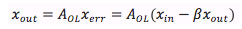
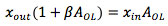
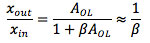
If A_OL is infinite, the relation between input and output is determined by beta only. In reality, A_OL is high, but not infinite, and, in addition, A_OL becomes smaller as the frequency rises. The piezo hysteresis and other errors result in an unwanted extra displacement delta under open loop conditions. These errors are reduced by negative feedback according to
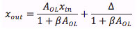
This means that the error is reduced roughly by the loop gain, which is the difference between the open and closed loop gain. If beta = 1, the full open loop gain A_OL is available to reduce the piezo hysteresis and other errors.
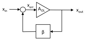
Figure 14. The 'excess loop gain' of the feedback loop is used to diminish the errors of the transfer function, including hysteresis. At higher frequencies, this gain is reduced to keep the loop stable
Common sensors for this purpose are e.g. strain gauges, variable capacitors and LVDTs (linear variable differential transformers). In the case of STM, the 'sensor' signal comes from the quantum mechanical tunneling current, and in the case of AFM from the displacement of a small cantilever beam. The sensors have to have very high accuracy themselves, and often sensor (or sensor preamplifier) noise dominates the position noise. But the most important disadvantage of a closed loop piezo system is the speed. Because it relies on negative feedback, there should be no large phase difference between the drive signal, what the piezo is doing, and the sensor signal. At higher frequencies the piezo response and the sensor signal will lag the input drive signal, and if this phase lag becomes too large, the closed loop system will oscillate. This places a limit on the gain-bandwidth, at the same time limiting the speed, and it also limits the curative properties of feedback as the frequency gets higher and higher. The latter is due to the diminishing open loop gain A_OL in the general feedback equation as the frequency rises to keep the amplifier stable; see [15] for details. Higher order compensation can reduce these disadvantages somewhat, but the 'gain should be less than one at 180 degrees phase shift' criterion still applies. A common higher order control scheme is the PID (proportional, integral and differential) controller, where the long term error and the edge response of a step signal are controlled individually, in addition to the proportional term of the equations above. Although the differential term of the PID can reduce the effect of the diminishing loop gain at higher frequencies and the correspondingly less perfect suppression of piezo hysteresis somewhat, a significant error will remain at high frequencies. This is why in the scanning probe microscopy field typically both the height image and the error image are recorded. The low frequency information is in the height image; the high frequency information is shared between both images.
Open loop compensation schemes that use certain prior knowledge about the piezo actuator system being driven are also used to speed up the system. Notably, one can design an electronic transfer function such that it mimics the inverse of the mechanical transfer function of the piezo. If the piezo is perfectly characterized and stable, this works well enough, but in practice, the high Q and slowly changing piezo properties limit the exactness of this approach. We will have more to say about this in Part II of this application note.
Piezo transformers are a special case in the piezo control loop business. In Fig. 15, it is shown that the electrical transfer function of a piezo transformer is not constant, but changes significantly with load. In addition, the resonance peak will also shift due to temperature changes and aging. At the same time the drive signal frequency needs to be locked to the resonance peak, and its amplitude controlled to such an extent that the output voltage of the piezo transformer is independent of the loading and resonance quality factor Q. There are also time delays along the mechanical path that prevent the possibility to create an oscillator circuit such as used for common piezo crystal oscillators. The way to do it is to not try to use the piezo transformer in an oscillator, but to let is output voltage drive a separate voltage controlled oscillator and resonant driver stage (Fig. 16) [6].
Figure 15. Electrical transfer function of a piezo transformer as a function of electrical load
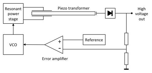
Figure 16. Recommended piezo transformer control loop solution. A resonant power stage (see Fig. 18) drives the piezo transformer. The output high voltage is rectified (with respect to ground, a single diode will not suffice due to the AC path), divided to the same voltage as the reference, and the error between the two amplified and sent to a voltage controlled oscillator (VCO). The VCO drives the power stage.
Piezo actuators are notoriously difficult loads to drive for a high voltage amplifier, even if the amplifier is called a piezo driver. The first point is that the piezo driver should be able to withstand voltages that are accidentally generated by the piezo itself and fed back to the driver output. If impact on a small piezo crystal is enough to create a spark to light up the cigarette lighter gas, it can be understood that the voltage and energy fed back from mechanical excitation of a piezo can be significant. It is always a good idea to be gentle while handling a piezo actuator, but especially so if it is connected to a piezo driver. Better disconnect the piezo from its driver before mechanical adjustments to the setup are made. Spurious voltages generated by the piezo under resonance conditions can also play havoc on a not-so-well-designed piezo driver output stage.
Below the resonance frequency, the piezo behaves as a high value capacitor, usually in the nanofarads to microfarads. They need to be steered by voltages between 50V and 1kV. Modern amplifiers (and piezo drivers are no exception) typically use negative feedback to obtain good specifications, such as low drift, precise amplification, low noise and distortion, and a high bandwidth. If these amplifiers are capacitively loaded at their output, the feedback loop will get an extra time delay, and hence phase shift, due to the low pas filter that is formed by the output impedance of the driver and the capacitance of the piezo. This phase shift may lower the feedback phase margin of the piezo driver, causing the driver to overshoot and ring with a sudden (step) change in voltage. Some commercial amplifiers have been known to become completely unstable with certain capacitive loads, resulting in outright oscillation.
Whether overshoots observed at the output of a piezo driver are caused by a low phase margin feedback loop, or by the piezo resonance itself, is often easy to determine. If the frequency of the overshoot is close to the resonance frequency of the piezo, it is the piezo resonance; if it is not, it is the amplifier feedback loop. Unless, of course, the two effects accidentally happen to occur near the same frequency, in which case extra care is necessary to unravel what is going on.
The Falco Systems piezo driver product range has features that prevent them from generating overshoot under capacitive loading conditions. Only the WMA-280 model is a 'normal' amplifier in this sense, and will show overshoot, while e.g. the WMA-100, WMA-200 and WMA-300 models will not. An application note detailing capacitive loading of piezo drivers called "High voltage amplifiers and the ubiquitous 50 Ohm: Caveats and benefits" is available here.
If high speed, high voltage amplitude operation is required, another factor comes into play. It takes a large current to charge a large capacitor to a high voltage quickly, by the defining equation of a capacitor C, with V the voltage, t time and charging current I

If the current required is larger than the maximum output current capability of the piezo driver, the maximum speed with which the voltage changes will be limited by the maximum current that the driver can sustain. This will lower the slew rate of the amplifier, defined as the maximum slope dV/dt with which the voltage at the output of the piezo driver can change, typically given in V/us. If the slew rate is insufficient for the intended output voltage amplitude at the intended frequency, the signal will be distorted as risetimes become longer. On a sine wave, this type of distortion is particularly easy to spot, as the sine wave will become progressively more 'triangle wave like' as the frequency is increased (Fig. 17).
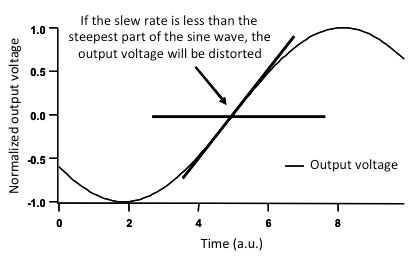
Figure 17. The minimum slew-rate required for a sine wave to be reproduced faithfully
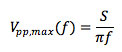
The maximum peak-to-peak sine wave output voltage V_pp,max at a frequency f that an amplifier with stated intrinsic slew rate S can provide without introducing slew-rate related distortion is
If the required output current is larger than the current limit of I_L ampere of the amplifier, again slew limiting will occur, but now at a lower slew rate S_I than the intrinsic slew rate of the amplifier, because the capacitance cannot be charged faster than with the maximum current available.

This lowered slew rate lowers the output voltage Vpp,max. An application note focusing on amplifier speed limitations including the slew rate and an online slew rate calculator, are available here, titled "High voltage amplifiers - How fast are they really?"
The stick-slip motor of Fig. 6 is one of the applications where a high slew rate is required. A rising ramp voltage slowly bends the piezo, but then suddenly the voltage steps back to zero, ideally at once. The required minimum slew rate for the step to 0V depends on the inertial moving mass and the maximum sustainable friction force on the contact between the piezo and its guide rails/walking surface. Here too, it is important to evaluate the maximum output current of the piezo driver and the piezo capacitance. This is to see whether the piezo will move with the speed of the intrinsic slew rate of the piezo driver, or with a lower, current-limited slew rate.
Some piezo driver manufacturers assume in their design that the piezo driver will only be required to supply the high current to prevent slew rate limiting during a small fraction of the time. This allows them to build an amplifier with a very high peak output current, without the added expenses required to build an amplifier with a high average output current. Such an amplifier cannot be used to create a large range continuous, fast periodic motion. It may be useful e.g. to drive a fast z-piezo in an AFM or STM to follow small features on the surface, where it encounters occasional 'bumps' on the surface where the piezo has to retract the fragile scanning tip quickly to prevent it from crashing into the surface, but otherwise is not required to deliver a lot of current. Another application can be the above-mentioned stick-slip motor in situations where the piezo capacitance is very high. If the average current rating of the amplifier is exceeded during such operations, the amplifier in question will suddenly either overheat, or reduce its maximum output current capability temporarily. Both will result in a change in amplifier output signal properties. In the case of an AFM or STM, e.g. a tip crash might result, or the stick-slip motor will not run anymore after some time. Sometimes a performance advantage can be had from an amplifier with a high peak-to-average current ratio. But because of this reason of varying properties of the output signal with use/time, Falco Systems only offers amplifiers where the average and peak current are the same. Such an amplifier will faithfully display the same behavior under all conditions, and will just as easily amplify a large amplitude square wave as a small irregular signal with occasional large excursions.
Many piezo actuators are predominantly used below the first resonance frequency, but others, such as ultrasonic resonant transducers, are meant to be used in resonance. In this case the drive requirements change significantly. At the mechanical resonance frequency itself, the piezo acts electrically as a pure resistance, i.e. voltage and current are in phase. This resistance is often low compared to the impedance of the capacitance at lower frequencies. This means that at resonance, a lower piezo driver voltage and a higher current are required than below resonance. Depending on the exact specifications, this signal can come from a similar piezo driver as discussed before. Using a generic, large bandwidth piezo driver in this situation is often interesting for low power applications and/or experimental setups. But in the final application it is more cost-effective to use a lower voltage, higher current narrow-band piezo driver, optimized for the piezo frequency in question. Such piezo drivers do not need to amplify DC and can advantageously use a step-up transformer to match the amplifier to the piezo (Fig. 18) impedance; they resemble switch mode power supplies in their operation and efficiency.
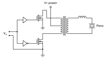
Figure 18. Cost-effective and energy-efficient piezo driver concept for driving a resonant piezo
Driving a piezo for fast precision positioning: damping the resonance
For fast, precise positioning systems, the sharp resonance of the piezo is a major limitation. It is common practice to just connect a piezo to a piezo driver and live with whatever shortcomings the combination of piezo and piezo driver may have in terms of resonances and piezo driver loading. But this is not the best way to do it. What we should be after, is to connect the piezo via a suitable coupling network such, that the piezo resonance is damped as much as possible, bandwidth is large, and the current required from the piezo driver is minimized. Although it may be counterintuitive at first, the piezo will have a high mechanical resonance peak if driven by a piezo driver that behaves as pure voltage source without series resistance. This is so, even though the voltage source keeps the voltage on the plates of the piezo accurately controlled, and no resonance peak is visible by looking at the voltage across the piezo.
The details of the electromechanical coupling between a piezo and its driver are presented in a separate Part II of this Falco Systems application note. It was already referred to earlier, and entitled "Optimal actuation of piezo's: electromechanical resonance damping in theory and practice". This second application note will be available here soon. In it, a comprehensive discussion of the passive damping of the first piezo resonance mode is presented, in electrical terms. This second application note on piezo's is necessarily more technical/mathematical in nature than the current Part I. Here, we only list its main conclusions, but we refer the interested reader to this second application note:
1. The piezo with its first (lowest) mechanical resonance can be modeled as an electronic circuit as given in Fig. 19. The mechanical response is equivalent to the integral of the current over time through the mechanical branch, defined by L_m, C_m, and R_m. C_o is the electrical capacitance as measured between the terminals of the piezo.
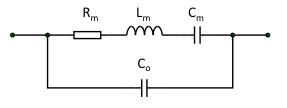
Figure 19. Equivalent schematic of a piezo with its first resonance
2. When the piezo is driven with a 'hard', low output resistance piezo driver, a large mechanical resonance (the 'primary resonance') is present in the response. This resonance is the series resonance caused by C_m and L_m. Its quality factor is determined by R_m. It cannot be seen by monitoring the voltage across the piezo, but the current drawn from the piezo driver becomes large.
3. If we place a large value resistor R_a in series with the piezo (Fig. 20), the bandwidth of the system is limited by the RC filter formed by this resistance and the piezo capacitance C_o. Instead of the primary resonance, there will be a another mechanical resonance (the 'anti-resonance') that is at a slightly higher frequency than the primary resonance. It is a parallel resonance including C_o. This resonance can be sharp (it has a high quality factor) but its absolute amplitude is lower than the primary resonance. The larger R_a, the sharper this resonance becomes. Its amplitude is always the same, if R_a is large enough, and independent of the exact value of R_a and the R_a*C_o-limited bandwidth.
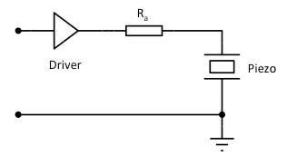
Figure 20. Piezo connected via a series resistance R_a
4. There is a 'midpoint' series resistance R_a,mid where the quality factor of the resonance is lowest. In this case the resonance frequency is halfway in between the primary resonance and the anti-resonance frequencies. The value of R_a,mid is
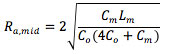
5. Although the quality factor of the resonance is lowest at R_a,mid, which is around 10 Ohm for most piezo's, the absolute magnitude of the resonance is lower still for slightly higher R_a values, where the resonance frequency approaches that of the anti-resonance, but the quality factor is still quite low. It is important to have some margin on R_a because of the significant changes of C_o with temperature and actuation voltage. For most piezo's the corresponding recommended value is around 50 Ohm, which is the output resistance of most Falco Systems piezo drivers, such as the WMA-100, WMA-200 and WMA-300 high voltage amplifiers.
6.A large current may flow through R_a. If R_a is implemented as a stand-alone resistor (as opposed to the internal resistor of the Falco Systems amplifiers), make sure that it is an appropriate high-power one. Because of the high frequencies involved, a thick film resistor is better than a wire-wound resistor.
7. More advanced compensation schemes have been described in the literature, notably the inclusion of an external inductor L_ext in series with R_a to create a series resonant circuit and short-circuit the remaining resonance peak (RL damping). The disadvantage is that only one value of L_ext and one value for R_a can be used: there is no room in this compensation scheme to employ the RC filter effect. Also, the circuit is much more sensitive to variations in the exact values of the components. Especially the variations of C_o with actuation voltage and temperature are so large that a passive RL damping is less effective than would be expected based on linear theory. Another possibility for extra compensation is to reduce the effect of C_o by the inclusion of a negative capacitance in parallel with the piezo. Because passive negative capacitances cannot exist, this approach requires an 'active' implementation with one or more extra high voltage amplifiers, configured as negative impedance converters (NIC). The added complexity and potential instability, and, again, the variability of C_o, limit the usefulness of this approach for most applications.
8. The final 'quick fix' recommendation is to at least include a resistor R_a in series with the piezo, with a value of a few times the calculated R_a,mid. A good value is usually around 50 Ohm, as implemented in the Falco Systems amplifiers. This solution will lower the piezo mechanical resonance significantly and is robust against variations in C_o. If the lower resonance peak near the anti-resonance frequency is still troublesome, it can be counteracted further by processing the input signal sent to the piezo driver with e.g. a computer implementation of the inverse (electrical to mechanical!) transfer function. This inverse transfer function approach only works well in practice if a significant series resistance R_a is present to lower the sharpness of the resonance peak first!
Conclusion
We have seen that piezoelectric actuators are based on crystals with an intrinsic dipole, and obtain their functionality from the internal charge distribution that changes under deformation. Piezo's come in many different forms and can be classified as linear mode, shear mode, tube, bending mode or MEMS respectively. There are many fields of application, and the wide applicability of piezo's has been illustrated with a number of important examples. For precision applications, we have covered the use of critically damped low-frequency second order external mechanical vibration isolation. Using the right amplifier and coupling network ensures that piezo positioning can be both fast and high resolution. It is important to use at least a high-power coupling resistor between a low output impedance piezo driver and the piezo itself to tame the mechanical resonances, as is implemented in the Falco Systems high voltage amplifiers. In Part II of this application note (a separate document that will be available here soon), the electronic damping of the piezo resonances is discussed in much more detail.
Acknowledgements
The author would like to acknowledge his (former) employers at IMEC vzw, Leiden University and Delft Technical University, his PhD students in Leiden and Delft, and the funding agencies STW (Veni and Vidi program) and FOM (free physics research program) for facilitating the work that laid the foundations for this application note.
Disclaimer and copyright
Although due care has been taken to ensure that the information contained in this application note is correct, Falco Systems does not assume any liability arising out of the application or use of any of the information described herein. Falco Systems reserves the right to make any changes to this application note without further notice. All text and images are (c) Falco Systems.
References
[1] R. M. Schmidt, G. Schitter, J. van Eijk, The design of high performance mechatronics, Delft University Press, The Netherlands, 2011
[2] Piezomechanics: an introduction, downloadable at www.piezomechanik.com, Piezomechanik
GmbH, Munich - Germany
[3] https://www.pifoc.com
[4] https://www.nanosurf.com
[5] F. Tabak, Towards high-speed scanning tunneling microscopy, Ph.D. Thesis, Leiden University, The Netherlands, 2013
[6] J. Williams and J. Phillips, Ultracompact LCD Backlight Inverters, Linear Technologies application note 81, 1999
[7] A. Camarda, G. Sordo, J. Iannacci, M. Schneider, U. Schmid, M. Tartagni, and A. Romani, Fabrication and alectromechanical modeling of a flexural-mode MEMS piezoelectric transformer in AlN, J. Microelectromech. Syst., Vol. 26, 2017, p. 1110
[8] https://www.memscap.com/products/mumps/piezomumps
[9] https://www.newport.com/c/optical-breadboards
[10] A. Gkouzou, Reducing nanoscale friction in multi-asperity contact systems: towards reliable MEMS devices, Ph.D. Thesis, Delft University of Technology, The Netherlands, to be published
[11] J. Kokorian, F. Buja, and W. M. van Spengen, In-plane displacement detection with picometer
accuracy on a conventional microscope, J. Microelectromech. Syst. Vol. 24, 2015, p. 618
[12] S.O. Reza Moheimani and A.J. Fleming, Piezoelectric transducers for vibration control and damping, Springer, London, 2006
[13] M. J. Rost, G. J. C. van Baarle, A. J. Katan, W. M. van Spengen, P. Schakel, W. A. van Loo, T. H. Oosterkamp, and J. W. M. Frenken, Video-rate scanning probe control challenges: setting the stage for a microscopy revolution, Asian j. Control Vol. 11, 2009, p. 110
[14] A. J. Fleming, Charge drive with active DC stabilization for linearization of piezoelectric hysteresis, IEEE Trans. Ultrason. Ferroelectr. Freq. Control Vol. 60, 2013, p. 1630
[15] J. K. Roberge, Operational amplifiers, theory and practice, J. Wiley and Sons, New York, USA, 1975